
Mastering iPhone Logic Board Diagnostics: A Comprehensive Guide to Chip-Level Troubleshooting and Micro-Soldering
iphone-logic-board-diagnostic-techniques-guide
The modern smartphone repair landscape has shifted dramatically over the last few years. Basic screen replacements and battery swaps are no longer enough to build a highly profitable repair business or secure a top-tier technician role. As smartphones become more compact and complex, the demand for technicians who understand circuit design, power management ICs (PMICs), and micro-soldering has reached an all-time high.
For repair technicians, electronics enthusiasts, and job seekers aiming to stand out in the competitive tech market, mastering iPhone logic board diagnostics is the ultimate technical skill. Unlike standard Android PCB layouts, Apple’s logic board architecture utilizes densely packed double-decker circuit boards, intricate communication buses, and multi-rail power distribution networks.
In this detailed technical guide, we will break down the essential diagnostic steps, specialized tools, and troubleshooting methodologies needed to identify and repair complex motherboard faults efficiently.
Understanding the Architecture of Modern iPhone Motherboards
To diagnose a dead or malfunctioning iPhone, you must first understand how electrical power and data flow through its logic board. Unlike basic single-layer PCBs, modern iPhones feature sandwiched mainboards connected via outer perimeter interposer pads.
The motherboard relies on several critical subsystem networks:
Main Power Rails (VCC_MAIN / VDD_MAIN): This is the primary power supply generated by the Power Management IC (PMIC) or Tigris/Hydra charging circuitry. A short on this rail brings down the entire device.
Battery Line (VDD_MAIN / V_BAT): Directly connects the battery connector to the primary protection MOSFETs and power ICs.
I2C and SPMI Data Buses: Inter-Integrated Circuit buses that allow the main CPU to communicate with sensor chips, display ICs, audio codecs, and camera modules. A pulled-down data line can cause boot loops (e.g., Error 4013 during iTunes restore).
Sub-Power Rails (Buck & LDO Outputs): Lower voltage supply lines created by the PMIC for specific subsystems like RAM, NAND storage, display backlight, and baseband.
When a device presents a “No Power” or “No Display” symptom, high-level technicians do not guess by replacing random components. Instead, they follow systematic electrical measurements.
Essential Hardware Diagnostics & Test Equipment
Executing professional chip-level repair requires high-precision lab equipment. Attempting logic board repairs with basic soldering irons can permanently damage multilayer trace lines.
Key equipment used in advanced training includes:
DC Power Supply (0–30V, 0–5A): Essential for checking boot current signatures and detecting subtle leakage currents before board startup.
Digital Multimeter (DMM): Must support fast Diode Mode readings and high-precision Resistance/Continuity testing.
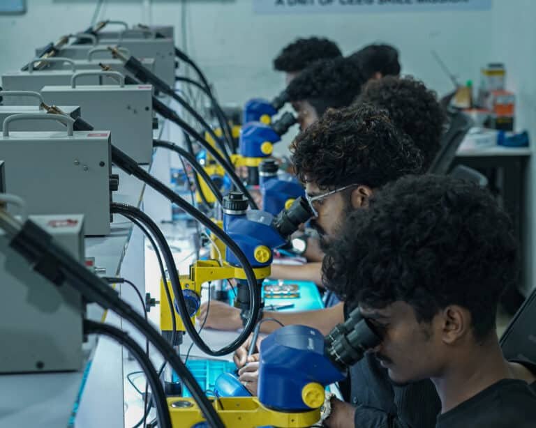
Trinocular Stereo Microscope: High-magnification optical inspection is crucial for viewing 0201-sized SMD capacitors, micro-junctions, and corroded trace lines under 45x magnification.
Thermal Imaging Camera / Freeze Spray: Quickly pinpoints shorted components by detecting localized heat generation when voltage is applied.
iBridge Test Cable & Schematics Software: Tools like ZXW, JCID, or Borneo Schematics provide real-time trace mapping, diode reference values, and interlinking pad connections.
Step-by-Step Diagnostic Framework for Logic Board Repair
Step 1: Initial Visual Inspection
Before applying power to a damaged logic board, conduct a microscopic inspection under warm lab lighting. Look for:
Liquid damage indicators (corrosion around backlight filter inductors and PMIC caps).
Physical micro-cracks on glass-encapsulated ICs.
Discolored solder joints or burnt trace paths resulting from high-voltage spikes.
Step 2: Diode Mode Line-Mapping
Diode mode measurement is the fastest way to detect open circuits (broken traces) or short circuits (ground faults) without powering on the board.
Connect the RED multimeter probe to ground (a copper shield or grounded standoff screw).
Touch the BLACK probe to the test points or component pins along the target circuit.
Compare your reading against known good board values in your schematics library:
OL (Open Line): Indicates a broken trace or disconnected filter bead.
0.000 V (Full Short to Ground): Indicates a shorted capacitor, diode, or internal IC silicon failure.
Deviated Values: A reading significantly lower than reference values indicates partial leakage or damaged silicon logic.
Step 3: DC Power Supply Boot-Up Amperage Analysis
Connecting the logic board to a regulated DC power supply yields a distinct amperage signature during the boot sequence:
0mA Draw (No Response): Broken power button trace, blown battery line MOSFET, or dead primary PMIC.
Instant High Amp Draw (e.g., 2.0A+ before pressing power): Direct short on the primary
VCC_MAINorVDD_MAINrail.Stuck at Low Current (e.g., 50mA – 80mA after power-on): CPU communication failure, corrupt NAND memory, or missing GPU core power rail.
Boot-Loop Amperage Pulse (0mA to 250mA cycling): I2C data bus short, damaged ambient light sensor flex, or missing battery data line (SWI).
Advanced Micro-Soldering Techniques: CPU, PMIC & Interposer Layering
Once a faulty IC or shorted capacitor is isolated, the repair phase requires expert-level soldering control.
Short Removal via Rosin Flux / Thermal Imaging
For a shorted capacitor hidden within a bank of decoupling capacitors, apply a small amount of liquid rosin vapor or view the board under a thermal camera. Apply a low voltage (1V–2V) matching the rail’s maximum rating using a DC power supply. The defective component will instantly vaporize the rosin coating or glow bright orange on thermal vision.
BGA IC Reballing and Replacement
Replacing modern BGA (Ball Grid Array) components requires strict heat and airflow regulation:
Preheating: Heat the entire logic board evenly to 100°C–150°C to prevent PCB warping.
Desoldering: Use a hot air rework station set to precise temperature and air-flow curves to safely lift the target IC without disturbing nearby underfill glue.
Pad Cleaning: Clean the underlying pads using solder wick and leaded solder alloy to lower the melting temperature.
Reballing: Apply high-purity solder paste through a precision steel stencil and apply uniform hot air until clean solder spheres form over the IC contact array.
Bridge the Skill Gap: Turning Technical Diagnostics into a Rewarding Career
As smartphones become faster and more intricate, repair service centers across India and the Middle East face a severe shortage of certified, skilled chip-level technicians. Learning standard hardware assembly is no longer enough to build a future-proof career; mastering diagnostic logic, schematics reading, and double-decker motherboard separation is what commands top industry salaries and opens doors to entrepreneurship.
At Nexgen Institute of Mobile Technology, hands-on technical training is at the core of every curriculum. Students train in modern, fully equipped repair labs utilizing real-world diagnostic tools, hot air stations, digital microscopes, and thermal imaging systems under expert mentorship.
Whether you are starting from scratch or looking to upgrade your existing repair skillset, explore our comprehensive training paths:
Master both Android and iOS board structures through our hands-on Courses program.
Learn about our industry-aligned curriculum, NSDC/STED government certifications, and practical lab facilities on our About Us page.
See how our alumni have successfully transitioned into certified technicians and business owners by reading our latest student stories on the Placements page.
Conclusion
Mastering iPhone logic board diagnostics requires a shift from superficial part replacement to structured electrical troubleshooting. By mastering multimeter readings, DC current analysis, schematics navigation, and precise micro-soldering, technicians can repair boards previously deemed irreparable. In a fast-evolving mobile economy, high-level chip diagnostics is not just a technical skill—it is a launchpad for long-term financial independence and professional growth.
Frequently Asked Questions (FAQ)
Q1: What is the difference between basic mobile servicing and chip-level repair?
Basic mobile servicing focuses on modular component replacements such as display screens, charging ports, batteries, and outer housing assemblies. Chip-level repair involves diagnosing motherboard circuits, replacing micro-SMD components, fixing short circuits, reballing ICs (Power IC, CPU, Audio Codec), and restoring broken PCB traces.
Q2: Do I need prior electronics engineering background to learn logic board diagnostics?
No prior engineering degree is required. With structured, practical training starting from fundamental electronics to advanced schematics reading, anyone with dedication and interest can become a proficient chip-level technician.
Q3: How long does it take to learn advanced iPhone chip-level repair?
At Nexgen Institute, comprehensive courses range from 4 to 8 months. Programs like our Professional Diploma in Advanced Smartphone & iPhone Chip-Level Training provide intensive practical lab sessions that take you from basic troubleshooting to advanced double-decker board separation and CPU reballing.
Q4: Are logic board diagnostic skills recognized with certification?
Yes. Completing chip-level programs at recognized institutions like Nexgen provides government-recognized certifications (approved by NSDC, STED Council, and Skill India), which significantly enhances job prospects in top service centers nationally and globally.
Contact Information
Ready to launch your career as a certified smartphone micro-soldering specialist? Connect with our admissions team today:
Institute Name: Nexgen Institute of Mobile Technology
Address: Second Floor, NKM Arcade, Ponnurunni, Vyttila, Kochi, Ernakulam, Kerala – 682019
Phone / WhatsApp: +91 90618 82000
Website: nexgeninstitute.in
Official Blog: nexgeninstitute.in/blog