
Comprehensive Guide to 5G Smartphone Hardware Diagnostics & Battery Drain Troubleshooting (2026)
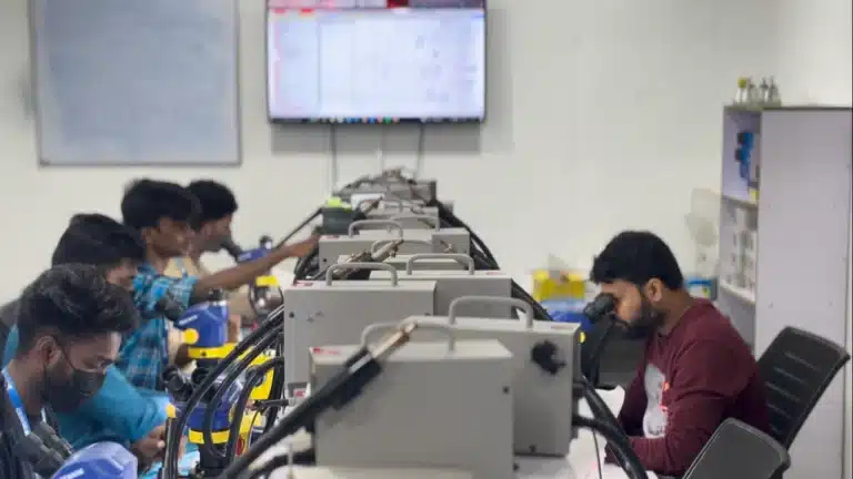
The rapid adoption of 5G networks across India, particularly in technology hubs like Kochi, has fundamentally transformed the smartphone architecture. While 5G provides ultra-fast data transmission and sub-millisecond latency, it also introduces significant hardware complexity. High-frequency RF transceivers, dedicated millimeter-wave (mmWave) antennas, multi-band Power Amplifiers (PA), and dual PMIC (Power Management Integrated Circuit) architectures now operate inside compact mobile chassis.
For modern mobile repair technicians, troubleshooting 5G smartphones requires moving beyond standard component replacement. Technicians must understand signal path analysis, power distribution network (PDN) short circuits, and thermal-induced power leakage.
In this comprehensive guide, we explore the step-by-step diagnostic workflow for identifying 5G hardware faults, fixing severe battery drain issues, and troubleshooting RF power leakage using professional chip-level diagnostic tools.
1. Understanding the 5G Hardware Architecture
To accurately diagnose a dead or malfunctioning 5G device, a technician must first understand how 5G hardware differs from older 4G LTE architectures.
+-------------------------------------------------------------------+
|                        5G Baseband Modem                          |
+-------------------------------------------------------------------+
                                  |
                                  v
+-------------------------------------------------------------------+
|               Sub-6 GHz & mmWave RF Transceiver                   |
+-------------------------------------------------------------------+
                                  |
       +--------------------------+--------------------------+
       |                                                     |
       v                                                     v
+-----------------------------+               +-----------------------------+
|    Low/Mid/High Band PA     |               |   Envelope Tracker (ET-IC)   |
+-----------------------------+               +-----------------------------+
       |                                                     |
       +--------------------------+--------------------------+
                                  |
                                  v
+-------------------------------------------------------------------+
|                   5G Antenna Matching Network                     |
+-------------------------------------------------------------------+
Key Components of 5G Circuit Boards:
Discrete 5G Baseband Modems & Integrated SoC Modems: Handles complex digital signal modulation and multi-gigabit throughput.
Sub-6 GHz & mmWave Transceivers: Transmits and receives ultra-high frequency radio signals, generating significant thermal output.
Envelope Tracking (ET) ICs: Dynamically adjusts supply voltage to the power amplifiers based on transmit power demands to maintain efficiency.
Multi-Phase Sub-PMICs: Works alongside the main PMIC to supply dedicated step-down voltages to high-current 5G processor cores and radio frequency power rails.
When any of these sub-circuits experience micro-shorting or capacitor breakdown, the smartphone exhibits symptoms like rapid battery drain, no service, low network signal, or severe thermal throttling.
2. Common Causes of 5G Hardware Faults & Battery Drain
Battery drain in 5G smartphones is rarely caused by a degraded battery cell alone. In 80% of chip-level diagnostic cases, the root cause is a secondary power rail leakage or a compromised RF power amplifier.
Primary Hardware Failure Categories:
Power Rail Capacitance Shorting (Main VDD / VPH_PWR Leakage)
SMD ceramic capacitors (MLCCs) filtering high-frequency ripple on 5G power rails deteriorate due to heat, causing micro-amps or milli-amps of parasitic current leakage even when the device is locked.
Overheated RF Power Amplifiers (PA IC Faults)
Continuous transmission on weak 5G signals forces the Envelope Tracker (ET IC) and High-Band Power Amplifier to operate at maximum output, leading to solder ball degradation or internal silicon breakdown.
Sub-PMIC Inductor Shorting & Thermal Runaway
High current demand on buck converters causes heat build-up around secondary power management ICs, leading to PCB layer delamination or flux resistance failure.
3. Step-by-Step Diagnostic Workflow for 5G Battery Drain
When a customer brings in a 5G smartphone reporting rapid battery discharge, overheating, or failure to charge, follow this professional chip-level diagnostic routine:
[ Step 1: Off-Board DC Power Supply Current Leakage Test ]
                           │
                           ▼
[ Step 2: Cold Checking via Diode Mode Multimeter Testing ]
                           │
                           ▼
[ Step 3: Thermal Camera Imaging & Rosin Atomizer Analysis ]
                           │
                           ▼
[ Step 4: Micro-Soldering BGA Reballing or Component IC Replacement ]
Step 1: DC Power Supply Static Leakage Analysis
Remove the battery and connect the device motherboard to a digital DC Power Supply set to 4.2V with a current limit of 3.0A.
Primary Leakage Inspection: Without pressing the power button, observe the ammeter:
0mA Reading: Main battery rail (VBAT / VPH_PWR) is clean.
Current Draw (e.g., 0.050A to 0.500A): Direct short circuit on the main input voltage line or primary PMIC input filtering stage.
Secondary Leakage Inspection: Press the power button once. Observe the boot sequence wave pattern:
If current spikes above 1.8A–2.5A during initial boot, a secondary voltage rail (BUCK convertor or LDO output supplying 5G modems) is shorted.
Step 2: Diode Mode Resistance Mapping
Using a digital multimeter in Diode Mode (Red probe on chassis ground, Black probe on test points):
Measure the ground resistance on key voltage supply rails:
VDD_COREVDD_MODEMS2_BUCK_1V2VREG_LDO_1V8
Compare your readings against standard reference motherboard values (ZXW or Borneo Schematics). A reading near 0.000V–0.020V indicates an active short on that specific power rail.
Step 3: Thermal Infrared Imaging & Short Isolation
Apply DC power to the shorted line using low voltage (1.0V–1.8V) high-current injection.
Utilize an Infrared Thermal Camera or apply rosin vapor across the suspected circuit area.
The shorted capacitor, Envelope Tracking IC, or 5G Power Amplifier will generate localized heat immediately, vaporizing the rosin coating or creating a high-temperature hotspot on the thermal imager.
+------------------------------------------------------------------+
|                    THERMAL IMAGING HOTSPOT MAP                   |
+------------------------------------------------------------------+
|                                                                  |
|   [ Main CPU / SoC ]          [ Main PMIC ]                      |
|       (32°C Normal)               (38°C Normal)                  |
|                                                                  |
|                                [ 5G RF PA IC ] <--- HOTSPOT!     |
|                                  (78°C FAULT)                    |
|                                                                  |
+------------------------------------------------------------------+
4. Advanced Micro-Soldering & IC Replacement Steps
Once the faulty 5G RF component or shorted ceramic capacitor is located, execution of micro-soldering precision repair is required:
PCB Securing: Place the logic board into a dedicated CNC microscope fixture.
Hot Air Rework Application: Pre-heat the board to 150°C using an under-board heater to avoid PCB warping. Set the hot air rework station to 350°C–380°C with medium airflow.
BGA Removal & Pad Cleaning: Remove the defective 5G IC or damaged SMD capacitor. Clean the pad array with desoldering wick and leaded solder flux to smooth out the BGA array.
Reballing & Alignment: Reball the replacement BGA IC using quality stencil and leaded solder paste (63/37 or Sn62/Pb36/Ag2). Align under a stereo microscope and apply hot air until solder surface tension centers the chip automatically.
Post-Repair Verification: Measure diode mode resistance again on the repaired line to verify the short circuit is completely cleared before powering on the device.
5. Practical Career Advantages of Master-Level 5G Chip Repair
As 5G smartphones dominate the consumer market, technicians with specialized chip-level repair skills enjoy a massive competitive edge:
Higher Repair Margins: Modern 5G logic board repair services yield significantly higher profits compared to simple screen or battery replacements.
Industry Demand: Certified technicians proficient in micro-soldering, schematic reading, and thermal diagnostics are highly sought after by premium service centers and international repair chains.
Entrepreneurial Independence: Master technicians can open independent advanced repair labs and handle outsourced board repairs for local repair shops across Kerala.
To build practical mastery on modern repair workstations and schematics, enrolling in a structured program like the Nexgen Institute Mobile Repairing Course provides real-world hands-on experience under expert guidance.
Conclusion
Mastering 5G smartphone hardware diagnostics, power rail troubleshooting, and battery drain identification is an essential skill set for modern mobile technicians in 2026. By following structured schematic analysis, diode mode testing, and precision thermal imaging, complex motherboard faults can be identified and resolved efficiently.
At Nexgen Institute of Mobile Technology, students receive comprehensive practical training in state-of-the-art diagnostic labs equipped with infrared thermal cameras, micro-soldering stations, and professional schematic tools. Whether you are aiming to secure high-paying jobs in authorized service centers or launch your own successful mobile repair business, our industry-recognized certification equips you with complete technical confidence.
Explore all career-oriented training options by visiting the Nexgen Institute Courses section and kickstart your journey toward becoming a certified chip-level mobile repair expert today.
Frequently Asked Questions (FAQ)
Q1: What causes battery drain in 5G smartphones even when not in active use?
A: Background battery drain in 5G smartphones is commonly caused by microscopic leakage in ceramic capacitors (MLCCs) on secondary power rails, damaged Envelope Tracking ICs (ET-ICs), or internal short circuits in the 5G Radio Frequency Power Amplifiers (RF-PA). These faults draw continuous parasitic current from the battery even when the screen is off.
Q2: Is advanced micro-soldering required for fixing 5G smartphone network and battery issues?
A: Yes. Modern 5G smartphones use high-density interposer board designs (sandwich motherboards) and micro-BGA chipsets. Resolving 5G hardware issues requires chip-level micro-soldering skills, BGA reballing, and proficiency with hot air rework stations and microscopes.
Q3: How long does it take to learn 5G smartphone chip-level repair at Nexgen Institute?
A: Nexgen Institute offers structured hands-on training courses ranging from 4 months to 8 months. Our Advanced Smartphone Chip-Level Training Course is designed to build complete practical competence from basic soldering to advanced 5G motherboard diagnostics.
Q4: Does Nexgen Institute offer practical lab practice on real 5G devices?
A: Yes. Students at Nexgen Institute work directly with modern diagnostic equipment, including DC power supplies, thermal imagers, digital oscilloscopes, and active 5G smartphone test boards under the mentorship of experienced instructors.
Q5: Can I open my own mobile repair shop after completing the course at Nexgen Institute?
A: Absolutely. In addition to expert technical and chip-level training, Nexgen Institute provides business guidance, tool setup consultation, and career support to help graduates establish and operate their own mobile repair business.
Contact Details
Institute Name: Nexgen Institute of Mobile Technology
Address: Second Floor, NKM Arcade, Ponnurunni, Vyttila, Kochi, Ernakulam, Kerala 682019
Phone / WhatsApp: +91 90618 82000
Email: nexgeninstitutecochin@gmail.com
Official Website: https://nexgeninstitute.in/
Explore Courses: https://nexgeninstitute.in/courses/
Read Our Blog: https://nexgeninstitute.in/blog/