
Mastering Smartphone Power Systems: Advanced Diagnostics for Power IC, Buck Rails, and Thermal Faults
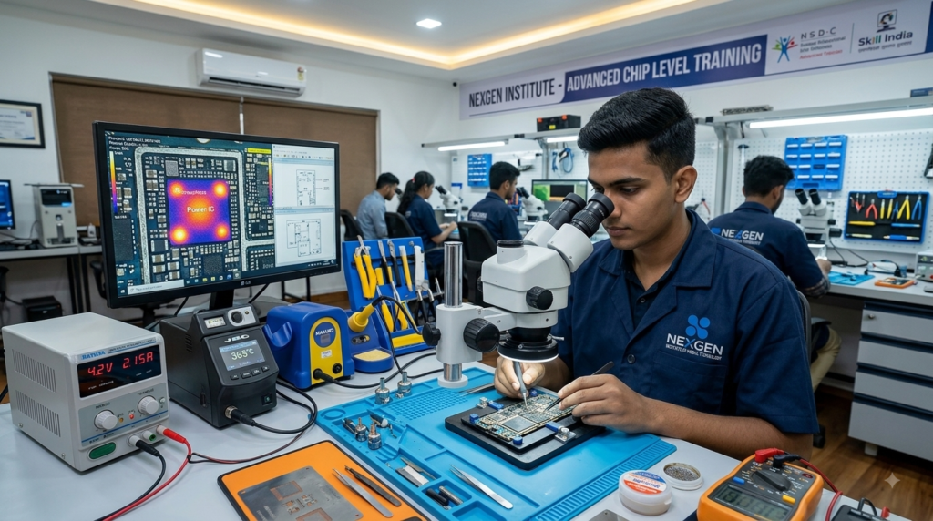
Advanced Smartphone Power IC & Thermal Diagnostic Masterclass | NexGen Guide
Modern smartphones pack immense computing power into ultra-compact, multi-layer printed circuit boards (PCBs). When a smartphone experiences sudden shutdown, failure to turn on, rapid battery drain, or severe overheating, the root cause almost always lies within the board’s Power Management Integrated Circuit (PMIC) or its associated energy distribution rails.
For modern mobile repair technicians, simple component swapping is no longer enough. To solve complex motherboard issues, you must master signal tracing, voltage rail testing, passive component testing, and thermal imaging.
In this comprehensive technical guide, we will break down the end-to-end diagnostic workflow for power-related smartphone failures, outlining the exact protocols taught in advanced chip-level labs.
1. Understanding the Smartphone Power Architecture
Before placing a probe on a logic board, a master technician understands how energy moves from the battery terminal to every integrated circuit on the board.
[Battery / USB Input]
         │
         ▼
[Primary Charging IC / OVP] ───► (Generates Main Power Bus: VPH_PWR / VCC_MAIN)
         │
         ▼
[Main Power Management IC (PMIC)]
         │
         ├──► Buck Converters (Low Voltage, High Current -> CPU, GPU, RAM)
         ├──► LDO Regulators (Clean Voltage -> Sensors, Cameras, Audio)
         └──► Sub-PMICs & Secondary Rail Distribution
The Three Core Power Bus Lines:
VBAT / VBUS: Direct voltage from the battery connector or USB charging port (3.7V – 4.4V or 5V/9V/12V fast charge).
VPH_PWR / VCC_MAIN: The main system power rail generated after the charging IC / Over-Voltage Protection (OVP) chip. This powers secondary components and the PMIC.
PMIC Output Rails:
Buck Regulators: High-efficiency step-down conversion delivering precise, high-amperage, lower voltages (e.g.,
0.8Vto1.2V) directly to the CPU Core and GPU.LDO (Low Dropout) Regulators: Low-noise filtered outputs supplying sensitive components like image sensors, touch ICs, and baseband chips.
2. Systematic Diagnostic Protocol: Step-by-Step Power Troubleshooting
When a dead device comes across your workbench, follow this sequential 4-step diagnostic protocol to isolate faults efficiently.
          ┌─────────────────────────────────────────┐
          │  Step 1: Visual & Chemical Inspection   │
          └────────────────────┬────────────────────┘
                               │
                               ▼
          ┌─────────────────────────────────────────┐
          │  Step 2: Diode Mode Line Resistance     │
          └────────────────────┬────────────────────┘
                               │
                               ▼
          ┌─────────────────────────────────────────┐
          │ Step 3: DC Power Supply Current Draw    │
          └────────────────────┬────────────────────┘
                               │
                               ▼
          ┌─────────────────────────────────────────┐
          │ Step 4: Thermal Camera / Rosin Tracing  │
          └─────────────────────────────────────────┘
Step 1: Visual & Chemical Inspection
Inspect the board under a High-Definition Stereo Microscope:
Check for liquid corrosion around line capacitors, buck inductors, and shield covers.
Inspect for physical cracks on micro-BGA chips or discolored/burnt MLCC (Multi-Layer Ceramic Capacitors).
Look for swollen board layers caused by thermal overload.
Step 2: Cold Diagnostics via Diode Mode
Using a digital multimeter set to Diode Mode (Red probe on Board Ground GND, Black probe on the test point):
Main VPH_PWR / VCC_MAIN Rail Check: Measure resistance to ground. Standard readings range between
0.300Vand0.550V. A reading under0.050Vindicates a full short circuit.Secondary Buck Rail Check: Measure output coils surrounding the PMIC. CPU power rails naturally read low resistance (e.g.,
0.015V - 0.080V), which is normal due to high internal CPU gate density. Do not mistake low CPU impedance for a hard short!
Step 3: Boot Current Analysis via DC Power Supply
Connect the motherboard to a regulated DC Power Supply (set to 4.2V with a 5.0A current limit) and observe the ammeter behavior:
| Ammeter Behavior | Indicated Fault | Recommended Action |
| Instant High Amperage Draw (> 2.0A) | Primary short on VBAT, VPH_PWR, or VCC_MAIN. | Perform voltage injection on the shorted rail. |
| Zero Current Draw on Power Button Press | Open circuit, broken power button flex, or PMIC boot pulse failure. | Check 1.8V PMIC wake-up voltage & crystal oscillator. |
| Stuck at Low Current (20mA – 80mA) | PMIC secondary buck line failure or corrupted bootloader firmware. | Check secondary LDO rails & force-flash system software. |
| Looping Current (100mA ──► 400mA ──► Reset) | CPU/RAM communication error, corrupted NAND flash, or I2C/I3S bus short. | Trace I2C pull-up voltages and inspect memory lines. |
3. Thermal Imaging & Rosin Flux Short Tracing
When a short circuit is present, current converts into thermal radiation. Modern technicians use two primary techniques to locate defective components rapidly:
               [ Inject Low Voltage into Shorted Rail ]
                                 │
                 ┌───────────────┴───────────────┐
                 ▼                               ▼
       [ Thermal Camera ]              [ Rosin Vapor Method ]
   (Real-time heat gradient)       (Visual melting point check)
                 │                               │
                 └───────────────┬───────────────┘
                                 ▼
                    [ Faulty Component Found ]
Thermal Imaging Cameras: Displays dynamic temperature changes across the PCB in real-time. A shorted capacitor or leaky silicon die will glow brightly within seconds of applying current.
Rosin Atomizer Technique: Smoke a light layer of rosin vapor onto suspected areas of the logic board. Inject voltage slowly into the affected power rail; the shorted component will instantly melt the white rosin layer, revealing the precise faulty capacitor or IC.
If you are looking to build a high-income technical career with hands-on exposure to these modern lab tools, explore our comprehensive Smartphone Chip-Level Training Courses designed for beginner and advanced students alike.
4. Protocol for Liquid-Damaged Logic Boards
Liquid intrusion causes rapid electrochemical corrosion (galvanic corrosion), forming conductive bridges across micro-capacitors and under BGA packages.
The Ultrasonic Decontamination & Rebuilding Procedure:
Immediate Power Isolation: Never attempt to power on or charge a water-damaged device before complete board cleaning.
Ultrasonic Bath Washing: Submerge the stripped board in high-purity Isopropyl Alcohol (IPA > 99%) or an engineered electronic cleaning solvent inside an industrial Ultrasonic Cleaner for 5–10 minutes to clear oxidized debris under BGA chips.
Bake & Dehydrate: Dry the board thoroughly in a temperature-controlled oven at 60°C–70°C for at least 30 minutes.
Capacitor & Rail Inspection: Check filter capacitors surrounding the backlight driver, display connector, and charging IC, as high-voltage lines suffer the quickest corrosion.
Micro-BGA Reballing: If corrosion penetrated beneath critical chips, remove the BGA package, clean board pads with solder wick, reball using precision stencils and flux, and reflow the chip accurately.
Learn more about our industry-leading practical methodology and world-class faculty by visiting About NexGen Institute.
5. Specialized Diagnostics: iPhone Logic Board Troubleshooting
Apple devices feature highly optimized logic board layouts with dual-layer sandwiched PCBs (iPhone X and newer). Troubleshooting these devices requires specialized diagnostic equipment and techniques:
┌─────────────────────────────────────────────────────────────┐
│                 iPhone Interposer Separation                │
├─────────────────────────────────────────────────────────────┤
│  Top Board: CPU, RAM, Power IC, NAND Flash, Audio          │
│  ─────────────────────────────────────────────────────────  │
│  Middle: Interposer Solder Joints (Reballing Frame)         │
│  ─────────────────────────────────────────────────────────  │
│  Bottom Board: Baseband RF, Wi-Fi, Bluetooth, NFC, Power     │
└─────────────────────────────────────────────────────────────┘
Interposer Separation & Testing: Utilizing pre-heating platforms set to precise temperatures (
180°C - 200°C) to separate top and bottom board layers, enabling independent testing of CPU and RF logic circuits.I2C / I3S Bus Diagnostics: Checking clock and data lines for pull-up voltage stability (
1.8V). A broken line on the I2C bus will prevent the CPU from communicating with power or display ICs, causing reboot loops.Panic Log Analysis: Reading built-in iOS panic logs (e.g.,
panic full) to instantly locate failing hardware sensors (such as charging flex thermal sensors, proximity sensors, or pressure sensors).
Interested in learning how our graduates achieve rapid job placement in top repair centers across the globe? Discover our stellar track record on our Placement Success Page.
Frequently Asked Questions (FAQs)
Q1: Can a faulty Power IC be repaired without replacing the entire chip?
In most cases, if the Power Management IC (PMIC) itself is internally damaged or shorted, it must be replaced with a compatible chip. However, often the fault is not the PMIC itself, but a shorted ceramic filter capacitor or inductor on one of its output rails. In those scenarios, replacing the tiny capacitor resolves the issue without changing the PMIC.
Q2: What equipment do I need to start performing chip-level power diagnostics?
To perform professional power diagnostics, your workbench requires:
A digital multimeter with fast continuity/diode testing.
A regulated 4-digit DC power supply (
0-30V / 0-5A).A high-resolution stereo binocular microscope.
A fine-tip temperature-controlled soldering station & hot air rework station.
A thermal imaging camera or rosin smoke atomizer setup.
Q3: What is the difference between a hard short and a soft short on a mobile motherboard?
Hard Short: Direct short circuit between a positive power rail and ground (
0.000Vdiode reading or 0 Ohms), causing high current draw immediately upon connecting power.Soft Short (Leakage): Partial line degradation or a damaged component pulling slight current (e.g.,
50mA - 150mA) only after pressing the power button or activating specific device features.
Q4: How long does it take to learn advanced chip-level micro-soldering and power tracing?
With dedicated hands-on practical training in fully equipped labs, students can master basic to advanced chip-level troubleshooting, BGA reballing, and schematic reading within 4 to 8 months.
Conclusion
Mastering smartphone power systems and board diagnostics transforms a routine technician into an in-demand micro-electronics specialist. By systematically applying diode mode measurements, DC boot current analysis, thermal imaging, and schematic tracing, you can confidently diagnose and repair even the most complex dead devices and water-damaged motherboards.
At NexGen Institute of Mobile Technology, located in Kochi, Kerala, we empower students with hands-on exposure to advanced tools, real device troubleshooting, government-approved certifications, and lifetime placement support.
Ready to level up your technical skills and launch a future-proof career in advanced mobile technology? Contact NexGen Institute Today to speak with our career counselors and reserve your bench in our upcoming practical training batch!